In the last post we learned about how to start a core development effort, and the importance of sourcing the real board and/or schematics to construct the FPGA model. Today, I will take you through the first steps of implementing the FPGA design by designing 2 key parts of the system: the MRA and the loader modules.
Conventions
First of all, it is important to note I follow some conventions I established in verilog for myself so that I can easily understand what is going on. I write module ports and parameters all as upper case (ie. CLK, RESET, DIN, DOUT). The reason why I do this is because it makes it easy for me to distinguish what is something that is internal to the module vs. external facing to other modules.
Second, I try to make the modules based on the high level block functions. I am not for creating an overly complex and abstract design where there’s multitudes of layers on top of each other. It makes it harder for me to create test benches and debug what is going on with the code. If there are smaller modules that I can implement to reduce repetitive logic, I will usually create that module in the same file.
The MRA
It is a good idea to start with the MRA as a first step. The MRA file will allow you to take a look at the files that are involved in the game rom and figure out their length and address mappings. For the purposes of this series, I will take you through the implementation of the Battle Garegga board, as it is the simplest of the 3 boards and the most straightforward to explain.
<misterromdescription>
<about author="pram0d" webpage="https://pram0d.com" source="https://github.com/psomashekar" twitter="@pr4m0d"/>
<name>Battle Garegga (Europe / USA / Japan / Asia) (Sat Feb 3 1996)</name>
<setname>bgaregga</setname>
<rbf>garegga</rbf>
<mameversion>0229</mameversion>
<year>1996</year>
<manufacturer>Eighting / Raizing</manufacturer>
<players>2</players>
<joystick>8-way</joystick>
<rotation>vertical</rotation>
<region>Europe</region>
<platform>Toaplan 2</platform>
<category>Shoot'em up</category>
<catver>Shooter / Flying Vertical</catver>
<mraauthor>pram0d</mraauthor>
<rom index="0" zip="bgaregga.zip" type="merged" md5="none" address="0x30000000">
        <!-- mapper for game 00 - bgaregga, 01 - sstriker, 02 - kingdmgp -->
        <part> 00 </part>
        <!-- maincpu -->
        <interleave output="16">
            <part name="prg0.bin" crc="f80c2fc2" map="01"/>
            <part name="prg1.bin" crc="2ccfdd1e" map="10"/>
        </interleave>
        <!-- audiocpu -->
        <interleave output="8">
            <part name="snd.bin" crc="68632952" map="01"/>
        </interleave>
        <!--  gfx1 -->
        <interleave output="16">
            <part name="rom4.bin" crc="b333d81f" map="01"/>
            <part name="rom2.bin" crc="b330e5e2" map="10"/>
        </interleave>
        <interleave output="16">
            <part name="rom3.bin" crc="51b9ebfb" map="01"/>
            <part name="rom1.bin" crc="7eafdd70" map="10"/>
        </interleave>
        <!-- extra text rom -->
        <part name="text.u81" crc="e67fd534"/>
        <!-- oki -->
        <part name="rom5.bin" crc="f6d49863"/>
    </rom>
<!-- Vertical game -->
<rom index="1">
<part>01</part>
</rom>
<switches default="00,00,00" base="8">
<dip bits="0" name="Test Mode" ids="Off, On"/>
<dip bits="1" name="Starting Coin" ids="1 Credit, 2 Credits"/>
<dip bits="2,4" name="Coin 1" ids="1 Coin/1 Credit, 1 Coin/2 Credits, 1 Coin/3 Credits, 1 Coin/4 Credits, 2 Coins/1 Credit, 3 Coins/1 Credit, 4 Coins/1 Credit, Free Play"/>
<dip bits="5,7" name="Coin 2" ids="1 Coin/1 Credit, 1 Coin/2 Credits, 1 Coin/3 Credits, 1 Coin/4 Credits, 2 Coins/1 Credit, 3 Coins/1 Credit, 4 Coins/1 Credit, Free Play"/>
<dip bits="8,9" name="Start Rank" ids="Normal, Easy, Hard, Very Hard"/>
<dip bits="10" name="Screen Flip" ids="Off, On"/>
<dip bits="11" name="Demo Sound" ids="On, No Sound"/>
<dip bits="12,13,14" name="Player Counts" ids="3, 4, 2, 1, 5, 6, Multiple, Invincible Mode"/>
<dip bits="15" name="Extra Player" ids="No Extra, 2000000 Each"/>
<dip bits="16,17" name="Region" ids="Japan, Europe (Tuning), USA (Fabtek), Asia"/>
<dip bits="19" name="Stage Edit" ids="Disable, Enable"/>
<dip bits="18" name="Continue Play" ids="Enable, Disable"/>
</switches>
<buttons names="Shot,Bomb,Formation,Coin,Start" default="Y,A,B,Select,Start" count="3"/>
</misterromdescription>The first section of the MRA is all metadata used to describe the game. The rbf here is important though, as that is what the core is named and what it looks for to run the game.
The second part, everything from the <rom> tag is used to describe the layout of the data you intend to send to your core to load and the composition of the data.
Lastly, the dipswitches and buttons are important as well as they describe the dips and inputs that are sent to the game core which your CPU will process.
Looking at this section of the rom organization, I will explain what each part means and why I have chosen this order to organize the data:
<rom index="0" zip="bgaregga.zip" type="merged" md5="none" address="0x30000000">
<!-- mapper for game 00 - bgaregga, 01 - sstriker, 02 - kingdmgp -->
<part> 00 </part>
<!-- maincpu -->
<interleave output="16">
<part name="prg0.bin" crc="f80c2fc2" map="01"/>
<part name="prg1.bin" crc="2ccfdd1e" map="10"/>
</interleave>
<!-- audiocpu -->
<interleave output="8">
<part name="snd.bin" crc="68632952" map="01"/>
</interleave>
<!-- gfx1 -->
<interleave output="16">
<part name="rom4.bin" crc="b333d81f" map="01"/>
<part name="rom2.bin" crc="b330e5e2" map="10"/>
</interleave>
<interleave output="16">
<part name="rom3.bin" crc="51b9ebfb" map="01"/>
<part name="rom1.bin" crc="7eafdd70" map="10"/>
</interleave>
<!-- extra text rom -->
<part name="text.u81" crc="e67fd534"/>
<!-- oki -->
<part name="rom5.bin" crc="f6d49863"/>
</rom>The layout of the data I will send is as follows:
- Byte 0x0: mapper code. The Garegga core plays 3 different games, and so in order to play multiple games with the same (but somewhat different) hardware design, you need a way to distinguish between them. I use this byte to set a register that is used as conditional logic. The core will take this and depending on the game, will run different sections or process different logic.
- Byte 0x1-0x100000: 68K program rom. Back in the days, EPROM chips were made in different sizes, and some were more expensive than others. Larger sizes of course were more expensive for a manufacturer to use. Secondly, the most common ROM chips had 8 bits for data output. That means that for each address you send over the address pins, you will only get 8 bits back at a time. The system design calls, however, for a 16-bit data output. That is to say, for a given address, you should get back 16 bits. In order to accomplish this, interleaving must be used. That is to say, on one chip, you have only the even bytes of the rom data, and the other chip will have the odd bytes. So, when you send a 16-bit address, you will get back 8 bits from rom chip 1, and 8 bits from rom chip 2. When you merge them together, you have the even and odd byte for that address, therefore making it 16.
- Byte 0x100001-0x120000: Z80 program rom. The system design calls for 8 bit data output from a rom chip connected to the Z80 CPU. So, no surprise, one rom chip, 8 bit addressing.
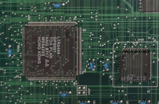
- Byte 0x120001-0x920000: Tile Graphics rom. The tile graphics are extensive and cover 0x800000 bytes total, or 8mb. No surprise, interleaving used here as well. However, the system design actually calls for 32 bit data output from these chips. So 2×2 are used in series and each chip/row has 16 bits of data output this time. 2 rows means a total of 32 bits can be achieved as an output per address. It is the M27C800 series in the Batrider schematic from last time, but a similar type of chip with the same pinout, but lower data space was used in Garegga. Due to the scheme of organization, a banking CPLD was used to retrieve the data from the right organization space in the rom chips.
- Byte 0x920001-0x928000: Extra Text rom. In Batrider and Bakraid, this is stored in the actual 68K program rom itself and unpacked by the 68k program rom pre-POST. However, in Garegga and earlier titles, it was included as an extra rom chip. This data concerns HUD elements and bitmap fonts used in the game.
- Byte 0x928001-A28000: PCM rom. All 3 games use ADPCM data which is processed by the M6295 (OKI) chip and the YMZ280B in Bakraid respectively. This is used to hold the PCM sample data which is decoded by the chip to play (usually) instrument and voice sounds.
How the Data is Sent
So now that we have the rom section figured out, all these bytes, in the locations listed above will be sent to your core, post interleaved, in order, 8 bits at a time. In the loading process, it is up to you to put the data somewhere as it comes in from the I/O ports on the MiSTer.
Where to put the data depends on how big the data is. You can certainly use an SDRAM controller and then load the data to SDRAM if it is large (as ours is). You may also use DDR which is on the stock DE10-nano. If it is small, you can also use the FPGA BRAM to store it. It is up to you.
For the purposes of our core, we will use BRAM to store the extra text rom and SDRAM for the rest of the data, and of course BRAM to store that one byte that’s the game selector byte.
I wont post the entire loader here. You can see the source here.
Constructing the ROM Map
To make life easier, I suggest you construct a ROM map. The relevant code is below:
parameter GAREGGA_ROM01_PRG_LEN = 25'h100000,
			  GAREGGA_ROMZ80_PRG_LEN = 25'h20000,
			  GAREGGA_GP9001_TILE_LEN = 25'h800000,
			  GAREGGA_TEXTROM_LEN = 25'h8000,
			  GAREGGA_PCM_DATA_LEN = 25'h100000,

			  KINGDMGP_ROM01_PRG_LEN = 25'h100000,
			  KINGDMGP_ROMZ80_PRG_LEN = 25'h10000,
			  KINGDMGP_GP9001_TILE_LEN = 25'h400000,
			  KINGDMGP_TEXTROM_LEN = 25'h8000,
			  KINGDMGP_PCM_DATA_LEN = 25'h80000,

			  SSTRIKER_ROM01_PRG_LEN = 25'h80000,
			  SSTRIKER_ROMZ80_PRG_LEN = 25'h10000,
			  SSTRIKER_GP9001_TILE_LEN = 25'h200000,
			  SSTRIKER_TEXTROM_LEN = 25'h8000,
			  SSTRIKER_PCM_DATA_LEN = 25'h40000
~~
~~
wire [24:0] ROM01_PRG_LEN = GAME == KINGDMGP ? KINGDMGP_ROM01_PRG_LEN :
							GAME == SSTRIKER ? SSTRIKER_ROM01_PRG_LEN :
							GAREGGA_ROM01_PRG_LEN,
		   ROMZ80_PRG_LEN = GAME == KINGDMGP ? KINGDMGP_ROMZ80_PRG_LEN :
							GAME == SSTRIKER ? SSTRIKER_ROMZ80_PRG_LEN :
							GAREGGA_ROMZ80_PRG_LEN,
		   GP9001_TILE_LEN = GAME == KINGDMGP ? KINGDMGP_GP9001_TILE_LEN :
							GAME == SSTRIKER ? SSTRIKER_GP9001_TILE_LEN :
							GAREGGA_GP9001_TILE_LEN,
		   TEXTROM_LEN = GAME == KINGDMGP ? KINGDMGP_TEXTROM_LEN :
							GAME == SSTRIKER ? SSTRIKER_TEXTROM_LEN :
							GAREGGA_TEXTROM_LEN,
		   PCM_DATA_LEN = GAME == KINGDMGP ? KINGDMGP_PCM_DATA_LEN :
							GAME == SSTRIKER ? SSTRIKER_PCM_DATA_LEN :
							GAREGGA_PCM_DATA_LEN;

wire [25:0] ROM_BASE = 26'h1,
		    SND_BASE = ROM_BASE + ROM01_PRG_LEN,
		    TILE_BASE = SND_BASE + ROMZ80_PRG_LEN,
		    TEXTROM_BASE = TILE_BASE + GP9001_TILE_LEN,
		    PCM_BASE = TEXTROM_BASE + TEXTROM_LEN,
		    ROM_END = PCM_BASE + PCM_DATA_LEN;

wire is_cpu = IOCTL_ADDR >= ROM_BASE && IOCTL_ADDR < SND_BASE;
wire is_snd = IOCTL_ADDR >= SND_BASE && IOCTL_ADDR < TILE_BASE;
wire is_tile = IOCTL_ADDR >= TILE_BASE && IOCTL_ADDR < TEXTROM_BASE;
wire is_textrom = IOCTL_ADDR >= TEXTROM_BASE && IOCTL_ADDR < PCM_BASE;
wire is_pcm = IOCTL_ADDR >= PCM_BASE && IOCTL_ADDR < ROM_END;
wire is_game = IOCTL_ADDR == 0;- The first part defines the length of each of the segments we need to load for all 3 games we support in this core.
- The second part maps those segments to a single net expression depending on the particular game detected in the first byte.
- Lastly, the third part is the ROM map that will allow us to detect when the IO is sending us data that is relevant to each of the sections. And, as those wires toggle, we can put the bytes in the relevant storage areas.
Now that we have a ROM map, we must define where we intend to put those bytes in our storage area of choice (ie. SDRAM):
localparam cpu_offs=0, snd_offs='h100000, pcm_offs='h120000;
wire [25:0] bulk_addr = IOCTL_ADDR;
wire [25:0] cpu_addr = (bulk_addr - ROM_BASE) + cpu_offs;
wire [25:0] snd_addr = (bulk_addr - SND_BASE) + snd_offs;
wire [25:0] pcm_addr = (bulk_addr - PCM_BASE) + pcm_offs;
wire [25:0] tile_addr = bulk_addr - TILE_BASE;
wire [25:0] textrom_addr = bulk_addr - TEXTROM_BASE; //this goes to a dpram
I use JT’s SDRAM controller, which has a banking system in place. There are 4 banks of memory in SDRAM with 32mb of total space. That means there are 8mb per bank you can use.
Because offsets have to be fixed for synthesis the way the modules are designed, I must establish fixed offsets at which to load part of the data that belong to the same bank of memory. This is the localparam offsets you see above (8-bit addressing, because our loader sends 8 bits at a time). I load all the graphics data cleanly in bank 1 by itself, so it needs no offset. Bank 0, on the other hand, contains the 68k program, the z80 program and the pcm data. Finally, BRAM contains the textrom, as we saw above.
This is the loader:
always @(posedge CLK) begin
    if(IOCTL_WR && !IOCTL_RAM) begin
		if(is_game) begin
			GAME<=IOCTL_DOUT;
		end else if(is_textrom) begin //textrom goes to dpram below.
			textrom_ldr_din <= {2{IOCTL_DOUT}};
			textrom_ldr_we <= ~IOCTL_ADDR[0] ? 2'b01 : 2'b10;
			textrom_ldr_addr <= textrom_addr>>1;
		end else begin
			PROG_WE<=1'b1;
			pre_data <= IOCTL_DOUT;
			pre_mask <= ~IOCTL_ADDR[0] ? 2'b10 : 2'b01;
			pre_addr <= is_cpu ? cpu_addr>>1 :
						is_snd ? snd_addr>>1 :
						is_pcm ? pcm_addr>>1 :
						is_tile ? tile_addr >>1 :
						'hxx;
			pre_ba <=  is_cpu ? 2'h0 : //cpu program
					is_snd ? 2'h0 : //snd program
					is_pcm ? 2'h0 : //pcm data
					is_tile ? 2'h1 : //tiles/gfx
					2'hxx; //nothing
			// $display("%h, %h, %h", pre_addr, IOCTL_ADDR, IOCTL_DOUT);

		end
	end else begin
		if(!DOWNLOADING || PROG_RDY) PROG_WE<=1'b0;
	end
end
as you can see, the conditionals will detect what parts of the rom are sent to us at any given time, and we can store them accordingly. There are a couple of things to note here:
- Since we are sent the data 8 bits at a time, and the SDRAM write affects 16 bits, we need to apply a mask for each write, so each write only can affect 8 bits either even or odd byte.
- Because our main data starts at an odd address, due to that GAME selector thing, we must apply the mask in reverse, otherwise the data will be offset by 1 byte, which is not correct (~IOCTL_ADDR[0]).
- As writes are done using a 16 bit addressing scheme, but we are sent data according to an 8-bit addressing scheme, we need to shift the address we intend to load to the sdram by 1 to the right (>>1).
That’s about it for the loader. When the system starts up, it will get the data from the SD card where the zip file is located, and pack the data according to the MRA into one contiguous file. Then, it will send us that data 1 byte at a time, and we simply can take the address its sending to us, and the data, and load it to the appropriate areas.
How to Access the Data
The JTFrame SDRAM controller has banks that are used to organize and retrieve the data accordingly. As mentioned above, I setup 2 banks. The first bank contains PCM, Z80 and 68K ROM, and the second, just the graphics. Finally, the text rom goes to a BRAM.
jtframe_rom_3slots #(
	.SDRAMW(22),

	.SLOT0_AW    (19), //68k rom (16 bit addressing)
	.SLOT0_DW    (16),
	.SLOT0_LATCH (1),
	.SLOT0_DOUBLE(1),

	.SLOT1_AW    (17), //z80 rom (8 bit addressing)
	.SLOT1_DW    (8),
	.SLOT1_LATCH (1),
	.SLOT1_DOUBLE(1),


	.SLOT2_AW    (20), //PCM rom
	.SLOT2_DW    (8),
	.SLOT2_LATCH (1),
	.SLOT2_DOUBLE(1),

	.SLOT0_OFFSET(0),
	.SLOT1_OFFSET(snd_offs>>1),
	.SLOT2_OFFSET(pcm_offs>>1)
) u_bank0 (
	.rst         (RESET),
	.clk         (CLK),

	.slot0_cs    (ROM68K_CS),
	.slot0_ok    (ROM68K_OK),
	.slot0_addr  (ROM68K_ADDR),
	.slot0_dout  (ROM68K_DOUT),

	.slot1_cs    (ROMZ80_CS),
	.slot1_ok    (ROMZ80_OK),
	.slot1_addr  (ROMZ80_ADDR ^ 1),
	.slot1_dout  (ROMZ80_DOUT),

	.slot2_cs    (PCM_CS),
	.slot2_ok    (PCM_OK),
	.slot2_addr  (PCM_ADDR ^ 1),
	.slot2_dout  (PCM_DOUT),

	.sdram_addr  (BA0_ADDR),
	.sdram_req   (BA_RD[0]),
	.sdram_ack   (BA_ACK[0]),
	.data_dst    (BA_DST[0]),
	.data_rdy    (BA_RDY[0]),
	.data_read   (DATA_READ)
);
`endif

//garegga's gfx is only 8mb, so only 1 bank needed.
jtframe_rom_4slots #(
    .SDRAMW      (22),
	.SLOT0_AW    (22), //gfx (8MB) (16 bit addressing, but the words are swapped.)
	.SLOT0_DW    (32),
	.SLOT0_DOUBLE(1),
	.SLOT0_LATCH (1),

	.SLOT1_AW    (22), //gfx (8MB) (16 bit addressing, but the words are swapped.)
	.SLOT1_DW    (32),
	.SLOT1_DOUBLE(1),
	.SLOT1_LATCH (1),

	.SLOT2_AW    (22), //gfx (8MB) (16 bit addressing, but the words are swapped.)
	.SLOT2_DW    (32),
	.SLOT2_DOUBLE(1),
	.SLOT2_LATCH (1),

	.SLOT3_AW    (22), //gfx (8MB) (16 bit addressing, but the words are swapped.)
	.SLOT3_DW    (32),
	.SLOT3_DOUBLE(1),
	.SLOT3_LATCH (1)
) u_bank1 (
    .rst         (RESET),
	.clk         (CLK),

	.slot0_cs    (GFX_CS),
	.slot0_ok    (GFX_OK),
	.slot0_addr  (GFX0_ADDR),
	.slot0_dout  (GFX0_DOUT),

	.slot1_cs    (GFXSCR0_CS),
	.slot1_ok    (GFXSCR0_OK),
	.slot1_addr  (GFX0SCR0_ADDR),
	.slot1_dout  (GFX0SCR0_DOUT),

	.slot2_cs    (GFXSCR1_CS),
	.slot2_ok    (GFXSCR1_OK),
	.slot2_addr  (GFX0SCR1_ADDR),
	.slot2_dout  (GFX0SCR1_DOUT),

	.slot3_cs    (GFXSCR2_CS),
	.slot3_ok    (GFXSCR2_OK),
	.slot3_addr  (GFX0SCR2_ADDR),
	.slot3_dout  (GFX0SCR2_DOUT),

	.sdram_addr  (BA1_ADDR),
	.sdram_req   (BA_RD[1]),
	.sdram_ack   (BA_ACK[1]),
	.data_dst    (BA_DST[1]),
	.data_rdy    (BA_RDY[1]),
	.data_read   (DATA_READ)
);

//TEXT ROM
jtframe_dual_ram16 #(.aw(14)) u_textrom(
	.clk0(CLK),
	.clk1(CLK),
    // loader
    .data0(textrom_ldr_din),
    .addr0(textrom_ldr_addr),
    .we0(textrom_ldr_we),
    .q0(),
    // Port 1
    .data1(16'd0),
    .addr1(TEXTROM_ADDR),
    .we1(2'b00),
    .q1(TEXTROM_DOUT)
);
There’s a couple things I want to explain about the options here. Firstly, each bank has 4 signals (CS, OK, ADDR, DOUT), and you will use these signals to get the data. CS is used to engage the bank, ADDR is used to send the address of the data according to the addressing DW defined in the parameters section (ie. 32, 16 or 8). OK is used to gate the data on your end when DOUT is valid and the data is retrieved. So, the process of getting the data is therefore as follows:
- CS set to high & ADDR sent.
- check for OK
- If OK, DOUT has your data.
Simple, right? Also note 1 quirk about this is the offsets I have in bank 0. Offsets are based on 16-bit addressing, so you need to shift right by 1 if you were using 8 bit addressing for your ROM map (as I am sure you were). That’s all, then send the signals out from your module and the other modules of your core can use them accordingly.
What’s Next?
Next, I will talk about the first module in the system to be created, which is the CPU module. Once you have the data, the next step is actually seeing if you can run the program for a target CPU and setting up the address bus, etc. which is the heart of the system. Thereafter, we will go into other subsystems like audio and graphics.
– pram0d